PCB is one of the types of parts that are used in electronic systems, especially electronic systems that have low voltage. Thick copper PBCs are types of PBs that are produced with special characteristics. We recommend you to continue with our Arya Madar Arjomand team to know more details of these products.
Thick copper PCBs
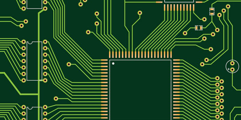
Thick copper PCBs are used in electronic systems and devices that have low voltage. PCBs are mostly used in high power devices and networks that have electrical conductivity with high current density.
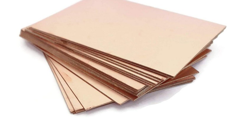
Different features of printed circuit board
Thick copper PCBs are one of the types of tools used in electronic devices. Due to their specific performance, these products have different features that we will mention below.
• These products have a high copper foil thickness.
• The thickness of PCB copper foils reaches more than 105 micrometers or even more.
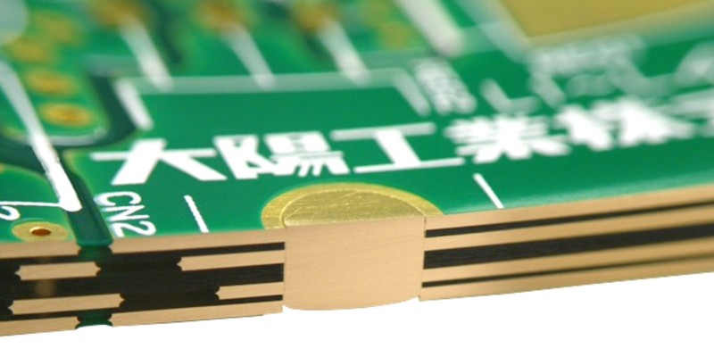
Important points about PCB
PCBs, which are made with thick copper, have different advantages and special design principles. In the following, we are going to mention the general information that will help you to design and produce the correct PCBs.
Various applications of thick copper printed circuit board
Thick copper PCBs can be single-layer, double-layer or multi-layer. Currently, PCBs produced in the form of circuit boards are used in power supply, management and distribution systems. These products can be used in aerospace or military industries. Among the various other applications that exist for thick copper PCBs, the following can be mentioned:
• Production of welding equipment
• Solar energy panels
• All types of power supply units
• Adapters and powerful converters
• Electrical engineering
• Automotive industry
• Railway industry
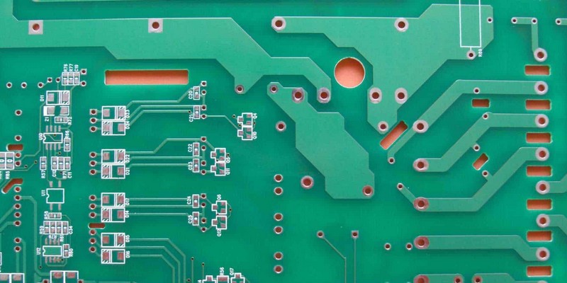
Advantages of thick copper PCBs
Due to the fact that these types of PCBs have different applications and are produced in a special way, they have gained special advantages. Among the advantages of thick copper PCBs, the following can be mentioned:
• It has excellent thermal and electrical conductivity
• Improvement of heat transfer along and on the PCB
• Reduction of disorders caused by inappropriate heat of PCBs
• Increase in thermal resistance and current carrying capacity in printed circuits
• Increase in the reliability of devices that are in the environment They work hard and at high temperatures.
• Increasing the mechanical resistance of contact points
Miniature planar transformer and its PCB application
Miniature flat transformers are one of the applications of thick copper PCBs. In these types of transformers, the windings are made on the PCB board as paths that are in the shape of a coil.
The windings are arranged around the slits that are next to the core, and the metal clamps make them secure. One of the advantages of this type of transformers is that by creating a flat arrangement on the coils, it prevents the cooling of the transformers. Therefore, it can increase the power efficiency of transformers.
Design of thick PCBs
One of the important issues that should be considered when designing PCB is the processing capacity of PCB manufacturers. Actually, it depends on the machines in the processing lines. The processing capacities define certain parameters that cause limitations for the allowed dimensions and the distance between their components. These parameters are called DRC parameters. These parameters increase by increasing the thickness of the copper foil.
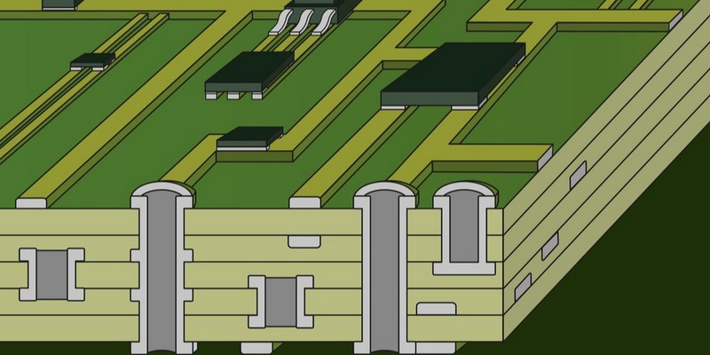
To design multi-layer PCBs, it is necessary to pay a lot of attention to the level of copper filling in the inner layers. If the copper filling level for the internal layers is 105 micrometers or more, we can prevent PCB delamination. For this reason, it is recommended that the types and number of thick copper PCBs be selected with the help of a software to help in the design of multiple layers.
Galvanic coatings that are placed on thick PCBs and have a conductive layer with a thickness of more than 105 micrometers, need 40 to 50 micrometers of copper compared to thin layers. This layer improves the mechanical strength of metal cavities, but it has one drawback. It may reduce the final diameter by more than 0.1 mm.
Another issue that should be taken into consideration for the use of thick copper PCBs is the significant increase of the PCB. Because in this case, a resistant layer is considered for soldering; Therefore, in this type of PCB, the final thickness is at least 0.25 mm more than the original thickness.
Conclusion
In this section, we explained the features of thick copper PCs, design principles, processing limitations, and the field of application of these PCBs. This information can reduce production costs in printed circuit boards. Choosing the wrong thickness of copper can affect the performance of the circuit assembly. Therefore, choosing the right thickness of copper is very important.